Optoelectronic Device Designer Panel
Design optoelectronic devices and plot the device energy level diagram.
To display this panel: click the Tasks button and browse to Materials → Tools → Optoelectronic Device Designer
The following licenses are required to use this panel: MS Maestro, MS Layered Device ML (optional), MS Informatics (optional)
- Using
- Features
- Additional Resources
Using the Optoelectronic Device Designer Panel
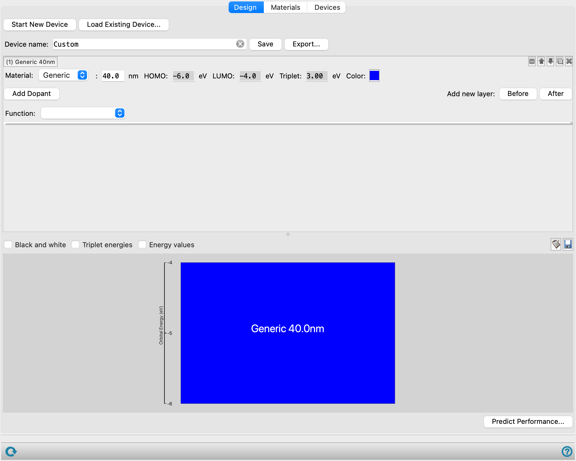
This panel allows you to design optoelectronic devices, such as Organic Light-Emitting Diode (OLED) devices, by building up layers using materials with known electronic properties and predict their performance. The panel displays the energy level diagram of the device, showing the HOMO and LUMO energy levels of each material in each layer, and optionally the triplet (T1) energy levels.
Common OLED materials and their relevant properties are available for use in the panel. Additional materials can be loaded into the panel using the Add New Materials button on the Materials tab. In the Optoelectronic Device Designer - Add New Materials Dialog Box, data from selected project entries is imported permanently into the panel for use in future devices. Each material added must have a HOMO, LUMO, and triplet energy level. These values can be taken from previous calculations using the Optoelectronics Calculations Panel or Machine Learning Property Prediction Panel, or the data can be entered manually when importing the materials. All materials are then available in the current and in future Maestro sessions.
Once a set of materials has been imported, devices are designed using the Design tab. The device is built layer by layer. For each layer, you must specify a thickness and host material. Additionally, any number of dopants and their concentrations can be specified. As layers and materials are added to the device, the energy level diagram is updated. Devices can be saved and are then available on the Devices tab in the current and in future Maestro sessions. Saved devices can be loaded into the Design tab for further editing using the Load Existing Device button. The current device diagram can be saved as an image, or the device recipe can be exported to a CSV file for sharing with other users.
The Devices tab shows a table with all saved devices. Additional devices can be imported from user generated CSV files or CSV files saved using the Export button in this panel.
The CSV file must contain a specific set of headers to be compatible with the panel. The file must specify a unique identifier for the device (ID) and the device formulation (Recipe). The recipe is space-delimited. Each layer is separated by a | (vertical bar) character. Within each layer, materials and amounts are given in pairs. The first material is the host and is followed by a layer thickness in nanometers. All following materials in a layer are dopants and are followed by a concentration. So a layer specified by BPHEN 15 BD1 5.00% has a thickness of 15 nm, BPHEN as a host, and BD1 as a dopant at 5% concentration. Material names must be names known to the panel (listed on the Materials tab either by name or alias).
An example data set could be formatted as follows:
ID,Recipe,Voltage@20mA (V),T50@20mA (H),T90@1mA (H),CIEx,CIEy,%NTSC,Brightness@20mA (cd),%EQE,T90@20mA (H)
OC1,HATCN 5 | NPB 40 | ALQ 30 BLALQ 15.00% | ALQ 40,,9.1,5000,9000,,0.42,10.,300.,3.1,400
OC2,HATCN 5 | NPB 40 | BPHEN 15 BD1 5.00% | ALQ 40 Li 1.00%,,,,,,,,,,,130
OC3,HATCN 5 | NPB 40 | BPHEN 15 BD1 8.00% | ALQ 40 Li 1.00%,,5.1,2000,3300,0.15,0.22,8.,220.,5.1,100
OC4,HATCN 5 | NPB 40 | BPHEN 15 BD1 10.00% | ALQ 40 Li 1.00%,,5.5,1700,3100,0.15,0.23,8.,250.,5.8,90
OC5,HATCN 5 | NPB 40 | BPHEN 15 BD1 15.00% | ALQ 40 Li 1.00%,5.9,2300,3500,0.15,0.22,8.,210.,4.9,120
where there are columns for the identifier (ID), device recipe (Recipe), and additional information about the devices(e.g.,Voltage@20mA (V),T50@20mA (H), %EQE, and so on).
To build and apply machine learning models for predicting OLED device properties, see the OLED Device Machine Learning Panel.
Optoelectronic Device Designer Panel Features
- Design tab
-
Define parameters for the layers of an optoelectronic device such as materials, composition, and thicknesses.
- Start New Device button
-
Use the Start New Device button to reset the panel to its default settings and clear any unsaved data from the Design tab.
- Load Existing Device button
-
Load a device from the saved devices set. Opens the Choose Existing Device dialog box where you can select sample devices L1-L6 that are included by default, as well as any devices you have previously saved.
- Device name text box
-
Specify a name for the current optoelectronic device.
- Save button
-
Save the current device with the specified Device name in the standard location in your Schrödinger user resources directory. The saved device is accessible through the Load Existing Device button.
- Export button
-
Export the current device to a CSV file. Opens the Export Device File dialog box so you can navigate to a location and name the file. This file can be loaded in using the Import devices button on the Devices tab. For more information on CSV files, see the Using section.
- Layer selection tools
-
These tools allow you to define the parameters for different layers for the optoelectronic device.
- Layer label
-
The label indicates the material and thickness of the layer. It is updated if either of the values are changed. The label remains visible when the layer settings are hidden.
- layer management buttons
-
These buttons perform display and ordering operations on the layer. They allow for easy duplication and rearrangement of layers.


Show or hide the contents of the layer. When hidden, only the layer number, label (if any) and these buttons are displayed. This is useful when you have a number of layers and want to compare two separate layers, for example. 

Move the layer up or down one place in the list. 
Duplicate the layer. This is useful for creating similar layers with variations on the settings. 
Delete the layer. - Material option menu and thickness/ percent composition text box
-
Select the material type from the provided options. See the Materials tab to view, edit, or add to the list of available materials. When you select a material, the label is updated with the material name, and its associated properties are displayed.
-
Additionally, specify the layer thickness for a specified host material, in nm, or specify the percent composition for a specified dopant material.
- HOMO text box
-
Displays the HOMO energy for the specified host or dopant material in electron volts. Noneditable.
-
See the Materials tab to view or edit the HOMO energy for a given material.
- LUMO text box
-
Displays the LUMO energy for the specified host or dopant material in electron volts. Noneditable.
-
See the Materials tab to view or edit the LUMO energy for a given material.
- Triplet text box
-
Displays the triplet state energy for the specified host or dopant material in electron volts. Noneditable.
-
See the Materials tab to view or edit the triplet energy for a given material.
- Color selector
-
Select the color of the host material or of the dopant material label. These colors are reflected in the device drawing.
- Trash icon
-
Click the Trash icon to delete the dopant from the layer. Only present if a dopant is added.
- Add Dopant button
-
Add an additional material to the layer at a given percentage. A new row of layer selection tools are displayed when this button is clicked.
- Add new layer buttons
-
Add another layer to the device before or after the current layer. Use the layer selection tools to define the new layer.
- Function option menu
-
Specify the function of the layer in the optoelectronic device. The menu items include Hole injection, Hole transport, Electron blocking, Emission, Hole blocking, Electron transport, and Electron injection. Functions must be specified for all layers in a device to use the Predict Performance button.
- Black and white option
-
Select this option to draw the device in black and white.
- Triplet energies option
-
Select this option to display triplet energies on the device drawing. An axis is added on the right-hand side to scale the triplet energy values.
- Energy values option
-
Select this option to display energy level value in eV next to each energy level line or boundary (including HOMO/LUMO and triplet energy levels) in the device plot.
- Copy image button
-
Copy an image of the device to the clipboard, so you can paste it into another application.
- Save image button
-
Save an image of the device to file. Opens a file selector in which you can browse to a location, select the image format (
.png), and name the image. - Plot area
-
Display the current device as layers stacked on one another. The layers are depicted as specified in the layer selection tools with the selected colors, specified thickness, and defined energy levels.
-
Clicking anywhere on a layer in the plot collapses all other layers in the layer selection tools rows above and opens the clicked on layer row. Text in the plot can be dragged to reposition it.
- Predict Performance button
-
Predict properties for the current optoelectronic device using ML models. Opens the Optoelectronic Device Designer - ML Predictions Dialog Box.
- Materials tab
-
View and edit materials available for device design.
- Add New Materials button
-
Add new materials for optoelectronic devices. Opens the Optoelectronic Device Designer - Add New Materials Dialog Box.
- Import Materials button
-
Imports materials from a CSV file into the Materials table. Click to open the Import Materials dialog box, where you can navigate to the file. The name of the file you selected is displayed in the text box.
- Materials table
-
Materials added using the Add New Materials button as well as preset materials are listed here. These settings define the properties of the given material and are used in the layer selection tools of the Design tab. Click on column headers to sort the data by alphanumerical value. Double-click on any cell to open a pane to edit the value. For the Triplet, HOMO, and LUMO values, the pane has an additional Source option menu to designate where the value was obtained.
-
Name—Specify the name of the material. Hover on any name to see the 2D structure.
-
Triplet— The triplet state energy for the material, in electron volts.
-
HOMO—The HOMO energy for the material, in electron volts.
-
LUMO—The LUMO energy for the material, in electron volts.
-
Aliases—Optionally specify one or more alternate names for the material. These names are then recognized when loading in new devices.
-
-
- Delete Selected Materials button
-
Removes all materials in rows that contain any selected cells from the Materials table. If any deleted materials are used by devices, those devices are also permanently removed. The Delete Materials dialog box allows you to confirm or cancel the deletion. If none of the selected materials to be deleted are used by devices the Delete material dialog box indicates the materials are safe to delete.
- Export All Materials button
-
Export all materials to a CSV file. Opens the Export Materials dialog box so you can navigate to a location and name the file. This file can be loaded in using the Import Materials button on the Materials tab.
- Devices tab
-
View and edit preset and saved devices.
- Import devices button
-
Load an optoelectronic device generated using the Optoelectronic Device Design panel and saved using the Export button on the Design tab. The device can be found in the working directory with the extension
-.csv. Click to open the Load Device File dialog box, where you can navigate to the file. The name of the file you selected is displayed in the text box. For more information on CSV files, see the Using section. - Devices table
-
Devices added using the Import Devices button as well as preset and saved devices are listed here. Click on column headers to sort the data by alphanumerical value. Double-click on any cell to edit its value.
-
ID—Device name from a preset, saved, or imported device.
-
Recipe— Details about the layers of the device.
-
Additional columns—Properties specified in the CSV file or predicted using the Predict Performance button.
-
- Delete Selected Devices button
-
Remove the selected row(s) from the Devices table. These devices are permanently removed from the list of stored devices.
- Export All Devices button
-
Export all devices to a CSV file. Opens the Export Devices dialog box so you can navigate to a location and name the file. This file can be loaded in using the Import Devices button on the Devices tab.
- Status bar
-
 to reset the panel to its default settings and clear any data from the panel.
If you can submit a job from the panel, the status bar displays information about the current job settings and status for the panel. The settings include the job name, task name and task settings (if any), number of subjobs (if any) and the host name and job incorporation setting. The job status can include messages about job start, job completion and incorporation.
The status bar also contains the Help button
 , which opens an option menu with choices to open the help topic for the panel (Documentation), launch Maestro Assistant, or if available, choose from an option menu of Tutorials. If the panel is used by one or more tutorials, hover over the Tutorials option to display a list of tutorials. Choosing a tutorial opens the tutorial topic.